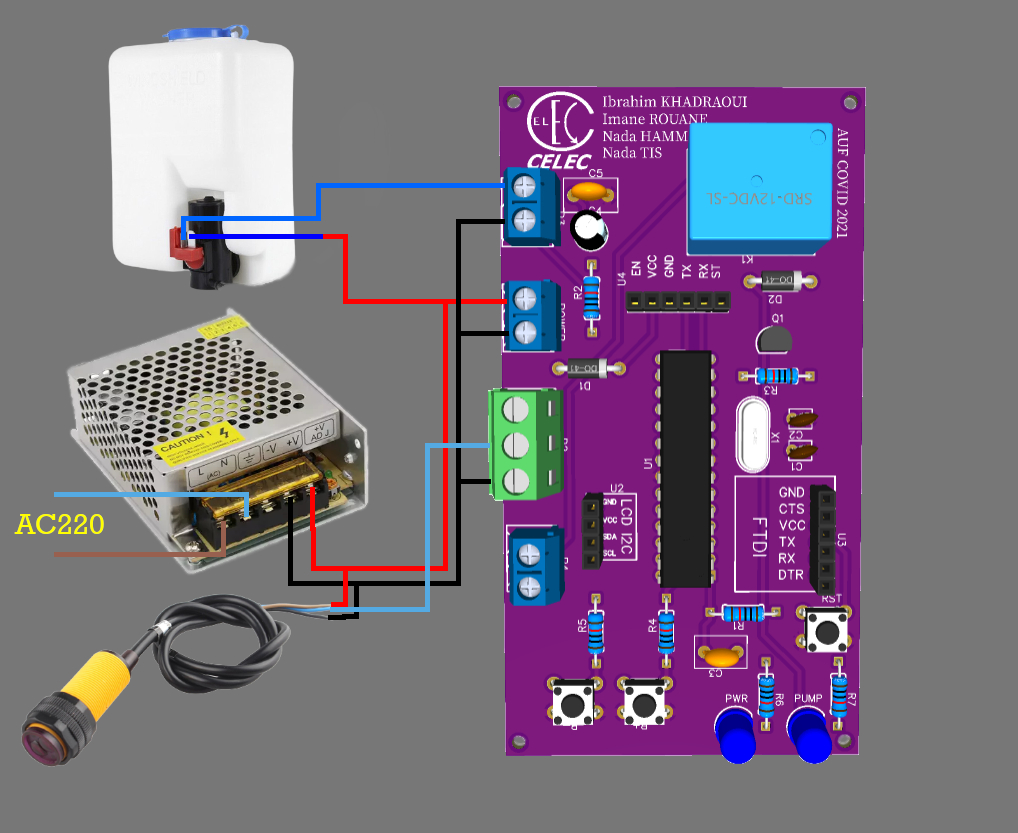
Other Projects Contactless hand sanitizer This board is based on an ATmega328P microcontroller, the E18-D80NK IR sensor detects the presence of a hand and sends a signal to the MCU which actuates the relay to run the pump for a short period of time to dispense disinfectant gel, the board also includes some additional options such as an additional input to place a level sensor to know the amount of gel at the level of the tank, the board also includes an input to place an LCD display via the I2C bus. Fast Line Follower (BATLFOLLOWER) This is my fast line follower I designed it from scratch, it’s based on an ATmega328P AU MCU. Odometer An electronic odometer to calculate distances, the device reads raw data from a sensor placed on the wheel of a car generally used for the ABS. Fast Line Follower (BATLFOLLOWER) This is my fast line follower I designed it from scratch, it’s based on an ATmega328P AU MCU. LORA RA-01 board carrier: A carrier board for the LORA RA-01 module, with a ON/OFF switch and a buck converter based on MP2307. Previous Post
Design of a wifi based device
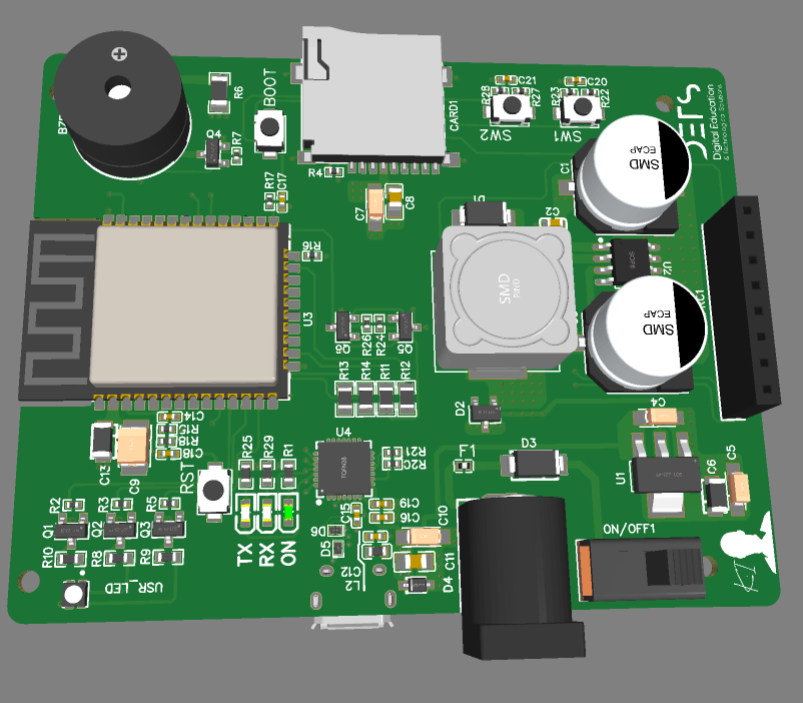
Design of a wifi based device In this project, I’m going to present to you the design of a PCB I made.For the first 4 layers PCB I made, I tried to use all I could acquire in the field of hardware design, thanks to the youtube channel of Robert Feranec who helped me so much to make this design. Presentation of the schematic The schematic is divided into four sections, starting from the top to the bottom, the power supply section, I used a cheap DC/DC converter to convert the 12V coming from the jack connector to a 3.3V, in the second section I put the SD card connector, an RGB led, a buzzer and a connector for placing an RFID module.In the third section, the ESP32 and all it’s must have component to work fine, and finally the USB to UART transceiver to upload code via USB and exchanging data and serial monitoring. The PCB The PCB is 4 layers and it’s 58x74mm, the top and bottom layers are signals and the inner 1 and 2 are ground and power planes, I placed the power section in the bottom far from the MCU and other IC’s because of the high frequency of the DC/DC converter. Previous Post
Building an Odometer for Cars Using ATmega328P-AU
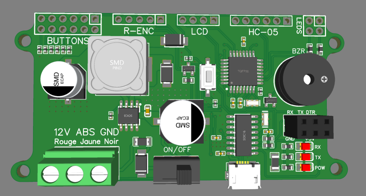
Building an Odometer for Cars Using ATmega328P-AU In this project, I designed an odometer that can be installed in a car. The odometer interfaces with the car’s ABS encoder to retrieve speed and distance data. This article details the design and implementation process, covering the schematic and PCB design. Overview The heart of the odometer is the ATmega328P-AU microcontroller (TQFP32 package). The power stage includes a DC/DC converter to step down the car’s 12V supply to 5V, ensuring stable operation for the circuit. Additionally, the board features a USB to UART transceiver for serial communication and monitoring via a computer. Tools And components ATmega328P-AU Microcontroller: This microcontroller is chosen for its versatility and compatibility with Arduino development environments, making it easy to program and debug. DC/DC Converter: The converter steps down the car’s 12V to 5V, providing a stable USB to UART Transceiver: Facilitates serial communication with a computer, allowing for monitoring and debugging. Schematic Design Microcontroller Section: The ATmega328P-AU is connected with essential components such as decoupling capacitors, a crystal oscillator, and pull-up resistors for the reset pin. Power Stage: The DC/DC converter is connected to the car’s 12V supply. The output is regulated to 5V, which powers the microcontroller and other peripherals. USB to UART Interface: The transceiver is connected to the microcontroller’s UART pins, enabling serial communication. Important Connections ABS Encoder Signal: The signal from the ABS encoder is fed into one of the ATmega328P’s input pins, allowing the microcontroller to process speed and distance data. Power Supply: Ensure proper connections and filtering to maintain a stable power supply and minimize noise. The PCB Overview The PCB design for the odometer is a two-layer board, measuring 41x82mm. It includes four screw holes for secure mounting. The layout is carefully planned to minimize electromagnetic interference (EMI). PCB Layout Power Section: Located at the bottom right of the board, the power section includes the DC/DC converter and associated components. Placing the power section separately helps in isolating noise from the digital components. Digital Section: Positioned on the right side, the digital section houses the ATmega328P-AU microcontroller and the USB to UART transceiver. This separation from the power section helps to reduce EMI. Ground Plane: A continuous ground plane is used to further minimize EMI and provide a stable reference for all components. Trace Routing: Critical signals, such as those from the ABS encoder, are routed carefully to avoid noise and ensure accurate data processing. Mounting Holes: Four screw holes are included to securely mount the PCB in the car. PCB Design Considerations Minimizing EMI: Separation of power and digital sections. Use of decoupling capacitors and proper grounding. Thermal Management: Ensuring adequate cooling for the DC/DC converter, especially in the automotive environment. Signal Integrity: Careful routing of critical signals to avoid noise and ensure reliable operation. Assembly and Testing Soldering Components Soldering Tips: Use a fine-tip soldering iron and quality solder. Ensure all components are properly aligned and soldered to avoid connection issues. Initial Power-Up: Connect the PCB to the car’s power supply and check for correct voltage levels and stable operation. Flashing the Firmware Programming the ATmega328P-AU: Use an Arduino-compatible programmer to flash the firmware onto the microcontroller. Ensure proper connections and follow the programming steps. Testing the Odometer ABS Encoder Signal: Connect the ABS encoder signal to the PCB and verify data reception using serial monitoring. Serial Communication: Use a terminal program on a computer to monitor and debug the data from the odometer. Conclusion This project demonstrates the design and implementation of an odometer for cars using the ATmega328P-AU microcontroller. By carefully designing the schematic and PCB layout, and considering factors such as EMI and thermal management, a reliable and functional odometer can be achieved. This project not only enhances understanding of microcontroller-based design but also provides a practical solution for automotive applications. Reference Documentation: ATmega328P Datasheet DC/DC Converter Specifications Further Reading: “Automotive Embedded Systems Handbook” by Nicolas Navet and Francoise Simonot-Lion “Practical Electronics for Inventors” by Paul Scherz and Simon Monk Previous PostNext Post
Testing Kicad6.0
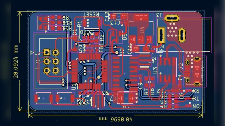
Testing Kicad6.0 Creating a learning PCB is an excellent way to deepen your understanding of electronics and embedded systems. In this project, we designed a PCB based on the STM32F103 microcontroller using KiCad 6.0. This board features a USB to UART interface using the CH340 chip, a 5V input jack connector, and a standard ICSP connector for debugging and flashing. Tools And components Software : KiCad 6.0 an open-source software suite for electronic design automation (EDA). Microcontroller: The STM32F103 series is a popular choice for learning and prototyping due to its powerful ARM Cortex-M3 core, abundant peripherals, and widespread community support. ICSP Connector Standard 6-pin ICSP connector for debugging and flashing the microcontroller. USB to UART Chip : CH340 The CH340 chip is used to convert USB signals to UART, facilitating easy communication with the microcontroller. Jack Connector for 5V Input : This provides a convenient way to power the board. Designing the PCB – Step 1: Schematic Design Creating the Schematic Starting a New Project: Open KiCad 6.0 and create a new project. Name your project appropriately. Adding Components: Add the STM32F103 microcontroller from the component library. Place the CH340 chip and connect it to the appropriate UART pins of the STM32F103. Add the 5V input jack connector and connect it to the power input pins. Include the ICSP connector and connect it to the debug pins of the microcontroller. UART Interface The USB to UART interface is essential for serial communication with the microcontroller. The CH340 chip is added to the schematic, with its USB pins connected to a USB port and its UART pins connected to the STM32F103. ICSP Connector The ICSP connector is critical for programming and debugging the microcontroller. Ensure all necessary connections to the STM32F103 are made, including power, ground, and relevant signal lines. – Step 2: PCB Layout Transferring Schematic to PCB Layout Importing the Schematic: Import the netlist generated from the schematic design into the PCB layout tool in KiCad. Component Placement: Place the components on the PCB canvas, considering signal flow and minimizing trace lengths. Routing the PCB: Route the traces, starting with critical signals like the clock and power lines. Use thicker traces for power and ground connections to handle higher currents. Design Rules Check (DRC): Run a DRC to identify and resolve any design rule violations. Generating Gerber Files: Generate the Gerber files required for manufacturing the PCB. Use a Gerber viewer to verify the files before sending them to the manufacturer. Manufacturing the PCB Choosing a Manufacturer : Select a PCB manufacturer based on factors like cost, turnaround time, and quality. Ordering the PCB : Follow the manufacturer’s guidelines to place an order. Ensure all necessary files (Gerber, drill files) are included. Receiving and Inspecting the PCB : Upon receiving the PCB, inspect it for any manufacturing defects. Check the alignment of the components and the quality of the traces. Assembly and Testing Soldering Components Soldering Tips: Use a fine-tip soldering iron for precision. Ensure proper solder joints to avoid connection issues. Soldering the CH340 and ICSP Connector: Solder the CH340 chip, ensuring all pins are correctly connected. Solder the ICSP connector for debugging and flashing the firmware. Initial Power-Up Connect the 5V input and power up the board. Check for any signs of short circuits or overheating components. Flashing the firmware Use the ICSP connector to flash the firmware onto the STM32F103. Follow the specific steps for your chosen programming tool. Testing the UART interface Verify the UART communication by connecting the USB port to a computer and using a terminal program to send and receive data. Debugging If any issues arise, check the connections and solder joints. Use a multimeter to verify continuity and proper voltage levels. Applications and future work Potential Applications This learning PCB can be used for a variety of projects, including: Embedded system prototypes Communication interfaces Sensor integration experiments Expanding the Design Consider adding features such as: Additional communication interfaces (I2C, SPI) More power supply options Onboard sensors or actuators Community and Learning Resources Join forums and communities related to STM32 and KiCad to share your experiences and learn from others. Utilize online tutorials and documentation to further enhance your skills. Conclusion This project provided a comprehensive overview of designing, manufacturing, and assembling a learning PCB using KiCad 6.0 and the STM32F103 microcontroller. By following this guide, you can create your own custom PCBs and advance your knowledge in electronics and embedded systems. Reference Documentation STM32F103 Datasheet KiCad Documentation Further Reading: “The Definitive Guide to ARM Cortex-M3 and Cortex-M4 Processors” by Joseph Yiu “Make: Electronics” by Charles Platt Previous Post


